/AI%20(artificial%20intelligence)/AI%20technology%20concept%20by%20NMStudio789%20via%20Shutterstock.jpg)
For decades, chipmakers have chased smaller and smaller transistors. But silicon — the material at the heart of every chip — has physical limits. With chips, going smaller and smaller becomes more and more difficult.
IBM (IBM) has just taken a big step forward in that regard. On June 25, the company unveiled the world's first sub-1 nanometer chip technology, operating at the 0.7-nanometer (7 angstrom) node. Here's what investors should know.
Why IBM's New Chip Architecture Changes Everything
IBM's sub-1nm breakthrough hinges on what IBM calls "nanostack," a completely new transistor design that stacks and staggers transistors in three dimensions. That's a notable departure from how chips have been built for years. Today's best chips use a flat, two-dimensional layout called nanosheet technology. IBM invented nanosheet, too — and now it's moving beyond it.
By going 3D, IBM can fit nearly 100 billion transistors onto a chip “the size of a fingernail.” That's roughly double the density of IBM's own 2-nanometer chip, which the company unveiled in 2021.
The performance gains are significant. Published technical results indicate that the new chip delivers up to 50% higher performance or up to 70% greater energy efficiency compared to IBM's 2nm chips, per the company's press release. That kind of leap matters enormously for artificial intelligence (AI) workloads, which require massive amounts of compute power and consume huge volumes of energy.
IBM Director of Research Jay Gambetta put it plainly. "With our new nanostack architecture, we're not just making smaller transistors, we're reinventing how chips are built to deliver dramatically more power and energy efficiency," Gambetta said in a company statement.
What Does This Mean for AI and Enterprise Computing?
Demand for compute power has never been higher. IBM Senior Vice President of Infrastructure Ric Lewis addressed that reality directly at the Bank of America 2026 Global Technology Conference in early June. He described an "AI lift" sweeping the entire industry, one that goes well beyond graphics processing units (GPUs).
"It's not all about GPUs. I would argue it's all about data. And that data needs to be moved. It needs stored, it needs fed, it needs processed," Lewis said at the conference.
IBM's new chip is designed to sit at the center of that need. Applications ranging from generative AI and cloud infrastructure to financial modeling and fraud detection all require faster, more efficient chips.
Lewis also noted that IBM's mainframe division, which runs its own custom chips, has seen its growth rate accelerate in recent cycles as AI workloads increase. IBM's sub-1nm chip fits into a much broader strategy the company is building around AI and enterprise computing.
In June, IBM announced partnerships with Alphabet's (GOOGL) Google Cloud and ServiceNow (NOW) as well as a tie-up with OpenAI's Daybreak Cyber Partner Program. In May, the firm also announced a $5 billion open source security initiative called Project Lightwell with Red Hat. All of these efforts are aimed at getting AI into production at scale inside large enterprises.
IBM's Semiconductor Road Leads to a Decade of Scaling
Beyond performance, IBM says nanostack architecture unlocks a path to continued chip scaling for at least another decade. Moreover, traditional chip scaling, following Moore's Law, has slowed, and industry observers are worried that the industry is running out of room to keep pace with demand.
IBM's research, presented at the VLSI 2026 conference, also showed that the nanostack architecture enables a 40% improvement in static random access memory (SRAM) density. SRAM is the fast memory built directly onto a chip, and more of it means better performance for data-heavy AI tasks.
The company's new chip is being developed at IBM's semiconductor research facility in Albany, New York. The site will soon house a High Numerical Aperture Extreme Ultraviolet lithography tool from ASML (ASML), a cutting-edge machine that prints the smallest possible circuit patterns.
IBM is working with partners — including Lam Research (LRCX), Tokyo Electron (TOELF), and SCREEN Semiconductor Solutions — on the next generation of manufacturing processes. The tech giant also recently announced Anderon, a standalone company that will serve as the world's first dedicated quantum-chip foundry, adding another dimension to its semiconductor ambitions.
The company sees a path to production for the sub-1nm nanostack technology within roughly five years.
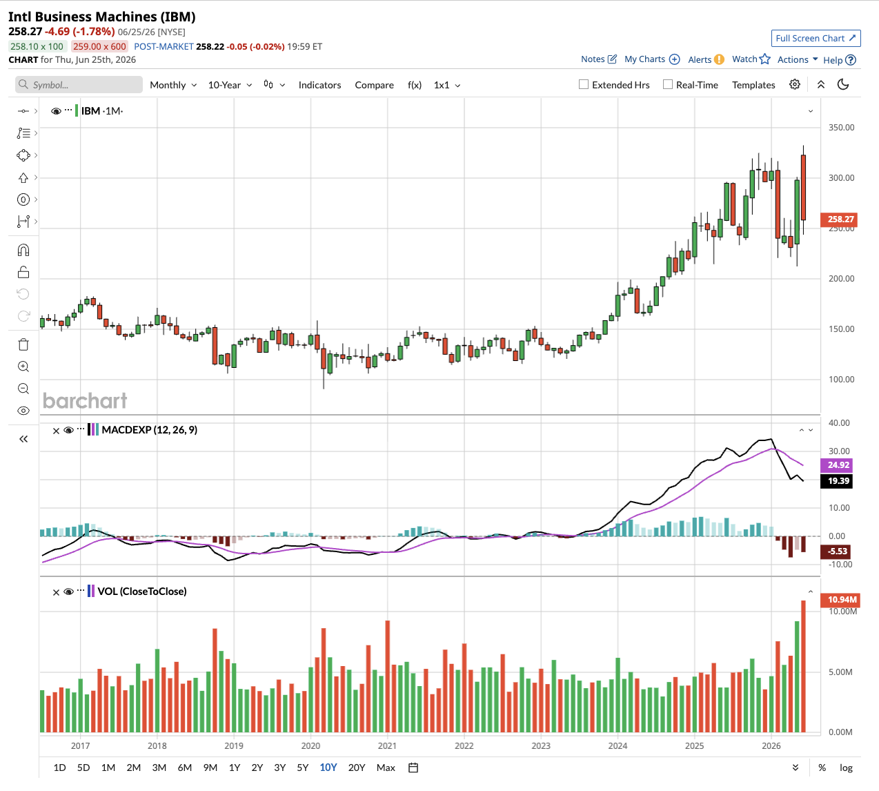
What's Next for IBM Stock?
Analysts tracking IBM stock forecast revenue to increase from $67.5 billion in 2025 to $85 billion in 2030. In this period, free cash flow (FCF) is projected to improve from $14.7 billion to $21.8 billion. If IBM stock is priced at 15 times forward FCF, which is similar to the current multiple, it could surge 45% from current levels within the next four years.
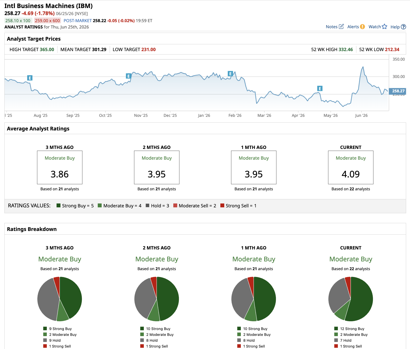
Out of the 22 analysts covering IBM stock, 12 recommend a “Strong Buy” rating, two recommend a “Moderate Buy,” seven recommend a “Hold” rating, and one analyst recommends a “Strong Sell.” The average IBM stock price target is $303.59, which implies potential upside of 9% from current levels.
On the date of publication, Aditya Raghunath did not have (either directly or indirectly) positions in any of the securities mentioned in this article. All information and data in this article is solely for informational purposes. For more information please view the Barchart Disclosure Policy here.


/An%20Intel%20sign%20out%20front%20of%20a%20corporate%20office%20by%20wolterke%20via%20Adobe%20Stock.jpeg)
/Alibaba%20by%20testing%20via%20Shutterstock.jpg)
/Alphabet%20(Google)%20Image%20by%20Markus%20Mainka%20via%20Shutterstock.jpg)