/AI%20(artificial%20intelligence)/Ai%20chip%20by%20Quality%20Stock%20Arts%20via%20Shutterstock.jpg)
Intel (INTC) is making its boldest statement yet that its chip manufacturing comeback is real.
At the 2026 IEEE/JSAP Symposium on VLSI Technology and Circuits, Intel Foundry confirmed that its Intel 18A-P process, the first performance upgrade to its flagship 18A chip family, has entered risk production. That means it is being manufactured in limited volume to validate yields and processes before full commercial rollout.
Intel has been under intense pressure to prove its foundry operations can compete with those of Taiwan Semiconductor Manufacturing (TSM) and Samsung.
Why Intel 18A-P Is a Big Deal for AI Chip Customers
Intel 18A was the first Intel process to combine two cutting-edge manufacturing techniques: gate-all-around (GAA) transistors and backside power delivery.
- GAA transistors wrap the gate material around all four sides of the current channel, improving control and efficiency.
- Backside power delivery moves the power wiring to the rear of the chip wafer, freeing up the front side for data signals.
- That combination is now the foundation Intel is building on with 18A-P.
According to a company statement, 18A-P delivers 9% higher performance at the same power level, or 18% lower power at matched performance, versus Intel 18A. For chip designers building artificial intelligence accelerators, mobile processors, or data center silicon, these are key numbers.
The process also introduces something Intel calls Power Boost, which it describes as the industry's first dual-contact architecture. It uses low-resistance connections on both the front and back of the chip, reducing electrical resistance for both NMOS and PMOS transistors. In plain terms, it lets more current flow through the transistor without the chip running hotter or consuming extra energy.
Thermal performance also improved, as Intel engineers reported 20 to 40% better thermal resistance across the overall chip stack, which is significant for dense AI workloads that generate significant heat.
Intel Foundry Is Ahead of Its Own Schedule
The progress on 18A-P fits into a broader pattern at Intel Foundry that has started to impress investors and customers alike.
Intel CFO David Zinsner, speaking at the Bank of America Global Technology Conference this month, confirmed that yield improvements on Intel 18A are ahead of the internal milestones the company set. He said Intel is now likely to pull in those targets by at least a quarter, and possibly more.
"Based on the progress we've made to date now, we are likely going to pull in those milestones by at least a quarter," Zinsner said.
Yield improvement is the primary driver of manufacturing profitability, and getting there faster than planned means Intel can quickly turn its foundry into a margin contributor rather than a drag.
Intel CEO Lip-Bu Tan has also been candid about the company's progress. At the JPMorgan Technology, Media, and Communications Conference in May, he said Intel is seeing roughly a 7% monthly yield improvement on 18A and is ahead of its year-end targets. He added that Intel 14A, the next-generation node after 18A, is already tracking ahead of where 18A was at the same stage of development.
What the Chip Science Showed at VLSI 2026
The research Intel presented at VLSI 2026 was notable for the level of detail and the silicon-validated data behind it.
On backside power delivery, Intel engineers showed that shifting power routing to the rear of the wafer cuts the routed block area by roughly 11%. It also reduces peak dynamic voltage droop from more than 90 millivolts on Intel 3 to under 10 millivolts on Intel 18A. That tighter voltage control translates directly into a 5-6% frequency boost, or up to 15% lower power, compared to chips using traditional frontside power networks.
Intel also showed CPU core results using GAA transistors with backside power. At a low operating voltage of around 0.5 volts, the GAA design ran roughly 30% faster than an equivalent FinFET design. That kind of low-voltage gain is critical for battery-powered AI devices and energy-constrained edge computing.
Beyond 18A-P, Intel presented early research on three technologies that point to its longer-term roadmap. Complementary FET (CFET) inverters with a 45-nanometer gate pitch offered a viable path to stacking NMOS and PMOS transistors vertically, pushing logic density beyond what GAA alone could achieve.
Subtractive ruthenium interconnects with air-gap integration reduce capacitance by up to 35% compared with copper, improving signal speed. And 300mm gallium nitride-silicon integration delivered more than 1,000 times higher power efficiency in logic circuits compared to previous GaN approaches.
Taken together, the VLSI presentations reinforced a simple but important message: Intel is investing seriously in the next three to five generations of process technology, not just the current one.
Is INTC Stock Undervalued Right Now?
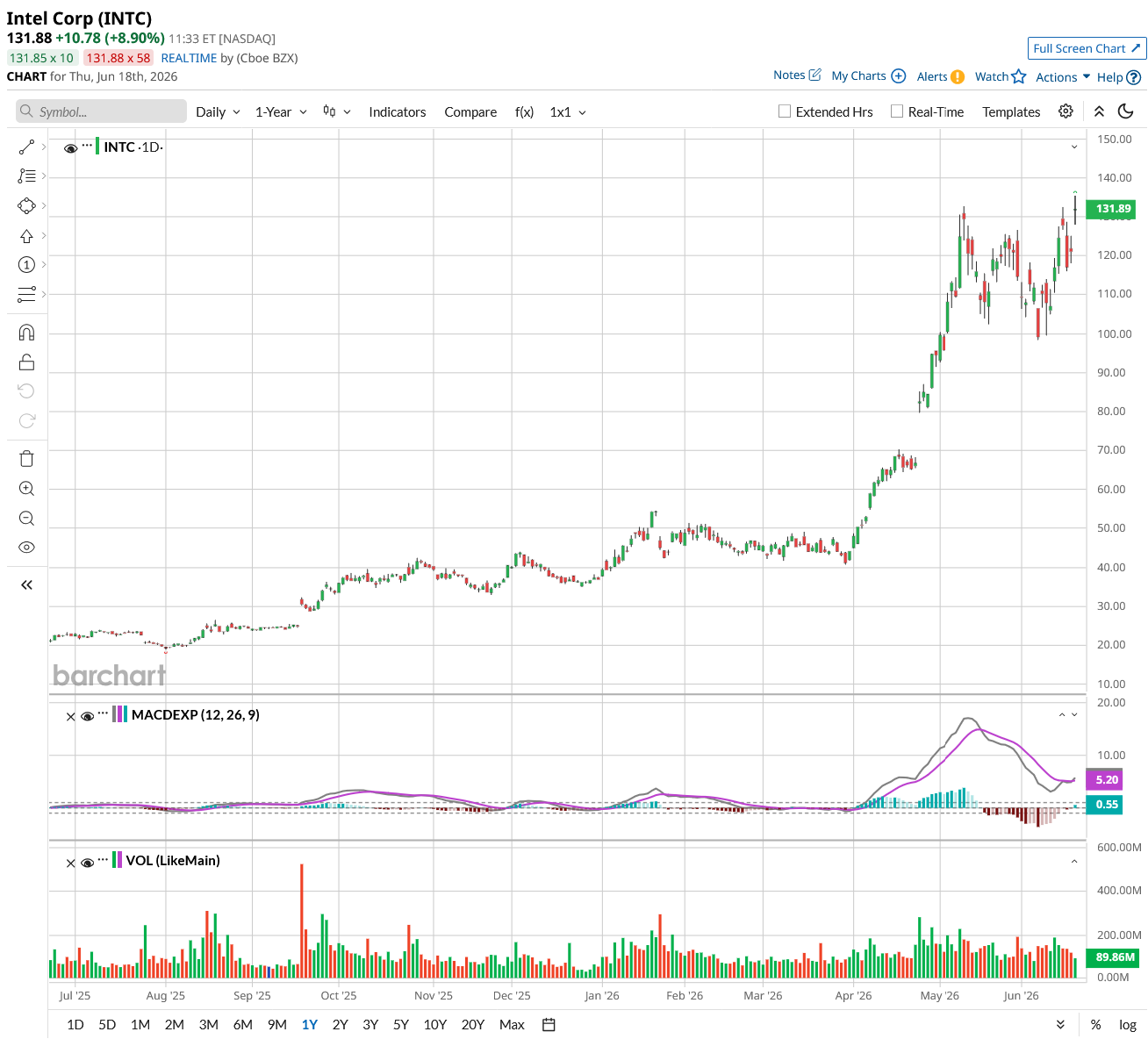
Valued at a market cap of $608 billion, INTC stock has returned over 500% over the last 12 months.
The semiconductor giant is projected to expand adjusted earnings per share from $0.42 in 2025 to $4.87 in 2030. If INTC stock is priced at 50x forward earnings, which is steep, it could roughly double within the next four years. However, if the earnings multiple “normalizes” to 30x, it could return just 20% by the end of 2029.
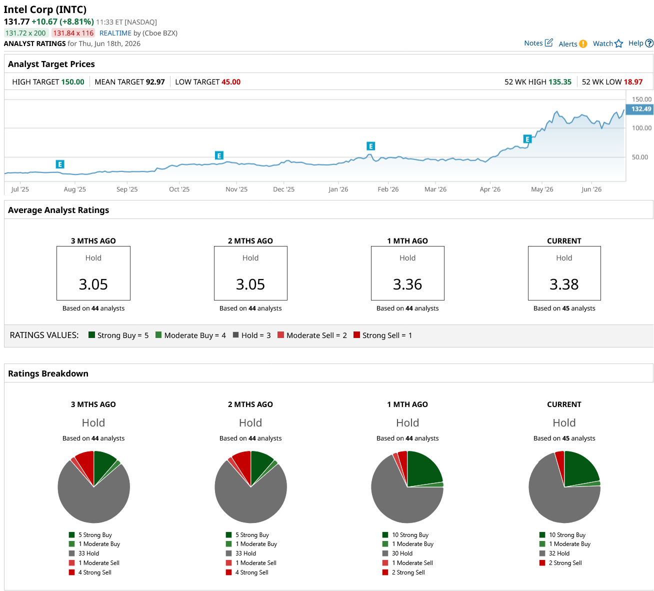
Out of the 45 analysts covering INTC stock, 10 recommend “Strong Buy,” one recommends “Moderate Buy,” 32 recommend “Hold,” and two recommend “Strong Sell.” The average stock price target is $92.97, below the current price of about $131.
On the date of publication, Aditya Raghunath did not have (either directly or indirectly) positions in any of the securities mentioned in this article. All information and data in this article is solely for informational purposes. For more information please view the Barchart Disclosure Policy here.

/A%20corporate%20sign%20for%20SK%20Hynix%20by%20Tada%20Images%20via%20Adobe%20Stock.jpeg)

/2d%20illustration%20of%20Cloud%20computing%20by%20Blackboard%20via%20Shutterstock.jpg)
/Server%20racks%20by%20dotshock%20via%20Shutterstock.jpg)